Inrush Current Limiter - Part2
Contents
In this article, I will concentrate on two ways to create a solid-state inrush current limiter circuit: One copies the relay-approach from Electronics knowledge: Inrush current limiters, just exchanging the relay with a p-channel MOSFET, and adding a more defined time delay. The other one has a “linear” approach turning power on gradually using a PNP power transistor.
Motivation: Inrush current limiter for USB-PD
As my experiments with USB-PD for AnywhereAmps failed, I have to create a circuit that limits inrush current to my amplifier before trying again.
Circuits explained
The two circuits are very similar. They only really differ in two components of the power section. Generally speaking, increasing delay capacitor C4 or increasing charge resistor R9 will prolong the delay time.
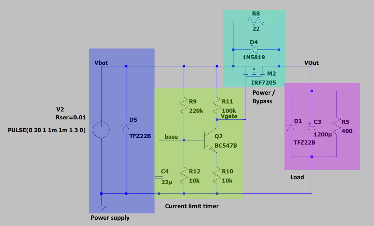
Input section (blue)
The input section features a transient voltage suppressor diode to eliminate reverse current or overvoltage cases.
Delay section (yellow)
When switched on, C4 will gradually charge via R9. When the NPN bipolar transistor Q2’s threshold voltage is reached, it will slowly reduce voltage behind R11 which will in turn activate M2, the power path of this circuit. R12 has been added to provide a stable operating point for Q2.
Power section (green)
The linear variant has a PNP power transistor Q1 in the main current path (image below). It is activated via Q2 and the current it can provide is controlled using R10, which in this case has a relatively low value to allow high emitter-collector currents.
While the switching variant uses a current limiting resistor R8 that is shorted by the p-channel mosfet M2, it’s voltage-controlled nature does not require special care when selecting R10. You should just make sure that it’s (negative) gate threshold voltage is well met.
Simulated load (purple)
My load is the power amplifier circuitry. To simulate its idle state and the powering-up behavior, I chose a 400Ohm resistor R5 and a 1200uF polarized capacitor C3. The TVS diode protects from over voltage and reverse currents. I have tried the simulations with capacitor values of up to 10000uF and resistors down to 40Ohm, all with similar and good results.
Circuit comparison
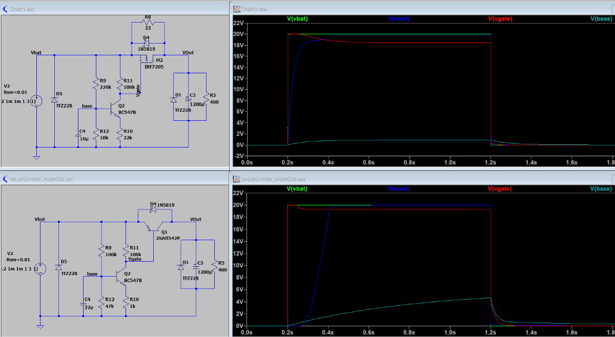 The blue line in the diagram is what is most relevant: It describes the output voltage of the system over time. Both circuits are tuned to reach target output voltage after 0.2 seconds. Still the curves differ quite a bit showing the different nature of the two approaches.
P-CH MOSFET approach
- Due to switching operation, inrush current limiter is effective but not exactly smooth
- power losses are very small for this variant because both triggering NPN transistor and power mosfet don’t use much power on their own.
- wide range of usability for connected devices only limited by the mosfet’s maximum continuous current.
PNP power transistor approach
- Very smooth operation, turn-on time can be controlled very well because of the PNP’s large ohmic region
- higher power losses when turned on due to high base current through
R10 - Not very versatile, as high load currents will create a considerable voltage drop over
Q1’s emitter-collector path.
Further improvements
To keep the versatility of this circuit high while at the same time keeping a smooth voltage curve, one could use an operational amplifier to monitor load current, regulating it down to allowed values if needed. The power mosfet could be kept while the disadvantage of the narrow ohmic operation band would vanish. The cost would be additional complexity like described in this electronics stackexchange post.