My Printed Circuit Boards arrived!
Sequel of Printed Circuit Board design blog entry
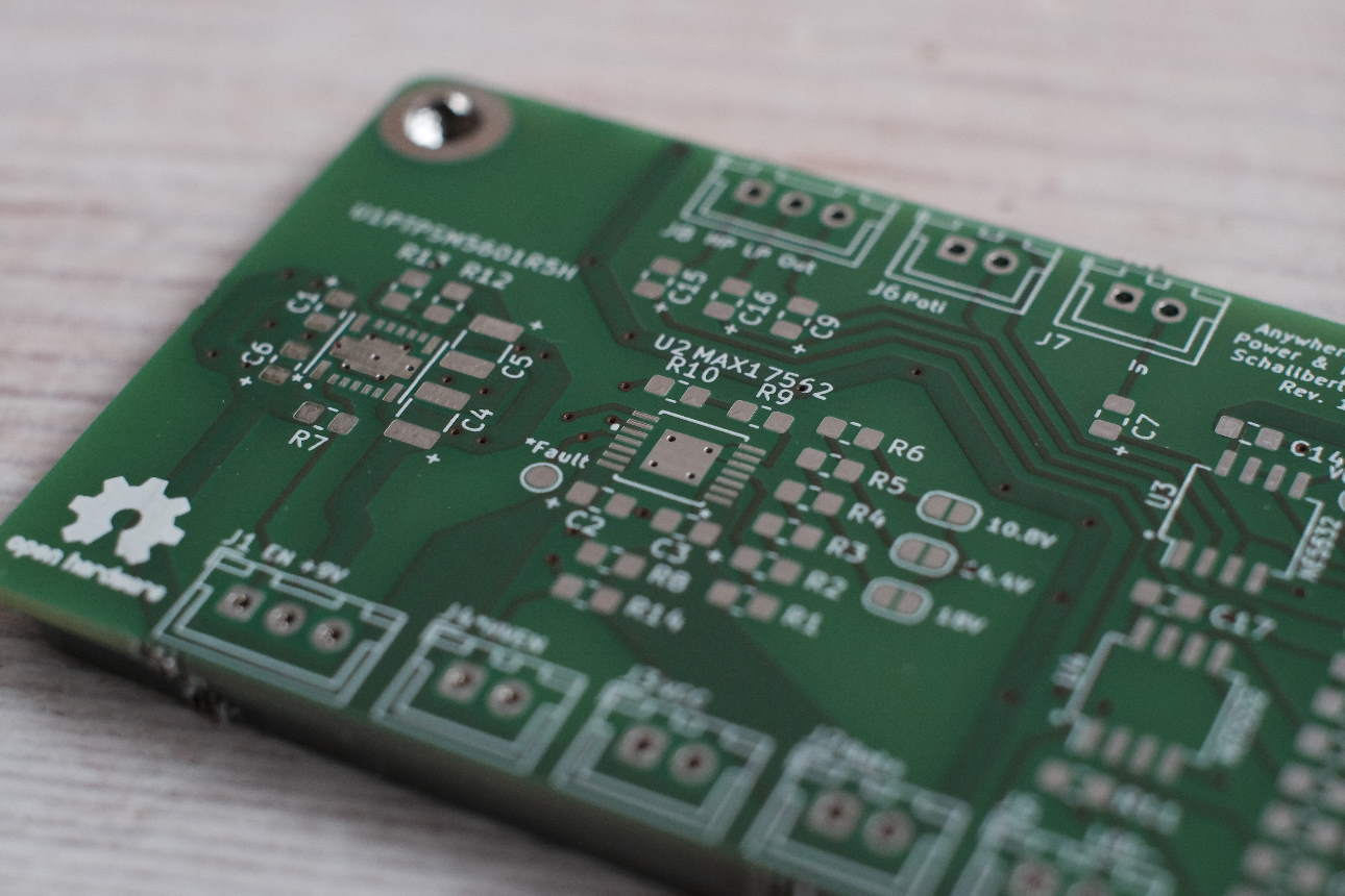
Arrival
After less than two weeks, my PCBs finally arrived along with all the parts needed to solder. I think they look beautiful :)
Soldering: Step-by-step
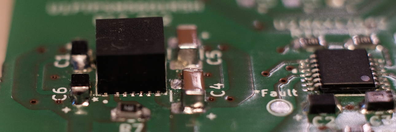
 I decided to solder the PCB in intervals, starting with the power management section. This way, I can test and correct the sections independently from each other. The SOIC (small outline integrated circuit) outline can still be hand-soldered easily when using lots of flux and a tool to “zoom in” for optical inspection. The only issue was that the IC has an “exposed pad”, i.e. there’s a ground pane on the bottom of the IC for better heat conduction. Soldering this was a nightmare. Finally I managed to fiddle solder through one of the bottom vias while keeping the iron at another via vor nearly a minute until it finally worked out fine.
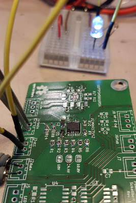
I’m pretty happy with the result, though. The system can be activated pulling *HVEN low, lighting up the LED. Tests for undervoltage/short circuit behavior went very well - the battery pack is protected now.
I decided to solder the PCB in intervals, starting with the power management section. This way, I can test and correct the sections independently from each other. The SOIC (small outline integrated circuit) outline can still be hand-soldered easily when using lots of flux and a tool to “zoom in” for optical inspection. The only issue was that the IC has an “exposed pad”, i.e. there’s a ground pane on the bottom of the IC for better heat conduction. Soldering this was a nightmare. Finally I managed to fiddle solder through one of the bottom vias while keeping the iron at another via vor nearly a minute until it finally worked out fine.
I’m pretty happy with the result, though. The system can be activated pulling *HVEN low, lighting up the LED. Tests for undervoltage/short circuit behavior went very well - the battery pack is protected now.
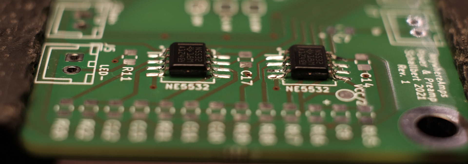
The Preamp section was easy to solder as well. Only the polarised capacitors proved to be so big that they covered much of the solder pad - this is a problem because the solder wouldn’t want to connect both cap and pad but just stick to one of these.
The 9V buck converter section - well… I didn’t manage to solder it by hand at all. Quadruple Flat Packs without leads (QFN) are hard enough, but this one has an exposed pad as well and I had to prepare much ground area to get the heat away from this component, so I couldn’t even get the temperatues high enough. So I borrowed a Hot Air station, and after some anxious trying and drowning the components in flux, I finally did it.
 I used my digital camera with a macro objective to inspect the solder connections.
Working
I build a lowpass and a highpass into the design to support 2-way speaker systems. To test the three preamp outputs (fullrange, lowpass, highpass), I directly connected the preamp to my speaker. It is not a good idea to do this, because the impedance of the speaker is far lower than the one of the OP-amp, so the output power is really low. Plus, the lower frequencies consume most power so the sound you hear is “high-pass” already and the low-pass volume is considerably less. Still, it works and I can adjust the gain as intended.
Preamp test
That’s it, my design is working! And remember, it is open source so you can download the project from my Github repository and order your own copy.
Lessons learned
Here’s the pitfalls and design flaws that should be corrected for Revision2:
- Prefer to place all components in the same direction (e.g. horizontally)
- Use thermal reliefs as much as possible to mitigate soldering issues due to thermal conduction
- Exposed pads: When hand soldering, the according solder pads must be extended to the sides of the IC for better solder heat conduction
- Avoid QFN footprints when hand soldering. They are a pain.
- If possible, don’t use footprint with “exposed pad” or “power pad”. A hot air station might be mandatory.
- Try to leave more space between component pads, esp. if placed horizontally.
- As SMD caps have more height, allow for bigger solder pads.